In today’s era of rapid technological development, every breakthrough in materials science brings new revolutions to numerous fields. Tungsten sputtering targets, as a key functional material, while less well-known, quietly drive progress in cutting-edge industries such as semiconductors, electronic displays, and optics.
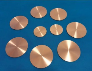
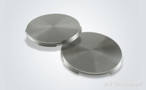
From the outside, a tungsten sputtering target appears to be nothing more than a dense, metallic disk or block, but the technological power it embodies cannot be underestimated. Its story begins at the atomic level. Tungsten atoms, with their unique structure and properties, are chosen to shoulder the heavy responsibility of building the microscopic “world of thin films.”
Tungsten stands out among metals with its astonishing melting point of 3410°C. This property makes it incredibly stable in high-temperature environments, providing a solid foundation for the sputtering coating process. When a high-energy particle beam, like a fine hail of bullets, whizzes towards a tungsten sputtering target in a vacuum, the tungsten atoms on the target’s surface are ejected one by one, breaking free from their original lattice constraints and scattering into the surrounding space. Like well-trained paratroopers, these atoms are precisely deposited onto the substrate, layer by layer, gradually building up a tungsten thin film with specific functions.
Tungsten sputtering targets play an indispensable role in the precision realm of semiconductor chip manufacturing. As chip manufacturing processes advance toward the nanoscale, circuit wiring becomes increasingly refined, making accurate and stable signal transmission critical. With its low resistivity, excellent electromigration resistance, and a thermal expansion coefficient that complements silicon-based materials, tungsten becomes the “invisible bridge” connecting chip components—the contact plugs and wiring. Every tiny tungsten atom deposited contributes to improved chip performance, driving electronic products towards faster, more powerful, and smarter advancements.
The electronic display industry is also a playground for tungsten sputtering targets. Tungsten thin film is present in the layers of coatings behind liquid crystal displays (LCDs) and in the critical coatings that ensure efficient and stable electrodes in organic light-emitting diode displays (OLEDs). Like an unsung hero, it precisely controls the reflection, transmission, and absorption of light by adjusting its thickness and microstructure, allowing us to enjoy a vibrant, clear, and smooth visual feast in front of our screens. Whether it’s the exquisite image quality of a mobile phone screen or the stunning visual experience of a large-screen TV, the silent dedication of tungsten sputtering targets is indispensable.
The manufacturing of optical devices is even more inseparable from the magical “magic” of tungsten sputtering targets. From the giant lenses of astronomical telescopes to the tiny objective lenses of microscopes, from the precision coatings of photographic lenses to the reflective mirrors of laser equipment, tungsten thin film acts like an “invisible armor” for optical components. Depending on the specific needs, this film can enhance reflectivity for more precise light focus or optimize transmittance for clearer images, opening new windows for those exploring the microscopic and macroscopic worlds.
Manufacturing a high-quality tungsten sputtering target is no easy task, much like meticulously carving a rare work of art. Powder metallurgy, from the initial tungsten powder screening and pressing to high-temperature sintering, requires strict control of process parameters at every step to create a target blank with a preliminary form. Subsequent precision machining ensures the target achieves the ultimate in size and surface flatness. Chemical vapor deposition, like “weaving a brocade” in the microscopic world, uses gaseous tungsten hexafluoride and hydrogen as raw materials. Under a specific temperature and pressure environment, tungsten atoms are deposited and grown like fine threads, producing high-purity tungsten plates of unimaginable purity and mirror-like uniformity. Further rolling, heat treatment, and other processes ultimately create a flawless tungsten sputtering target.
Looking back on the development of tungsten sputtering targets, they have advanced alongside technological advancements, and market demand has snowballed. Global tech giants and material manufacturers are fiercely competing for their research and development and production. From inheriting advanced processes from Japan, to innovative explorations in Europe and the United States, to the vigorous pursuit of domestic companies, each technological iteration has written a legendary chapter in the struggle of materials science.
Looking ahead, with the in-depth development of cutting-edge technologies such as 5G, artificial intelligence, and quantum computing, the performance requirements for tungsten sputtering targets will inevitably reach new heights. Higher purity, more sophisticated microstructures, and properties more adaptable to complex processes will become new research and development directions. They will continue to be hidden behind technological products, illuminating innovations for humanity through atomic deposition in the microscopic world, steadily advancing toward an uncharted new technological journey.
Keywords:
TUNGSTEN TARGET,tungsten sputtering targets,tungsten thin film