Molybdenum Sputtering Targets
FOTMA’s high-purity molybdenum sputtering targets are widely used in the following areas:
- Semiconductor Industry: To create barrier layers, contact layers, and thin-film transistors.
- Optical Coating: For the production of optical reflection films, anti-reflection films, and filters.
- Solar Cells: Used as back electrodes and conductive layers.
- Flat Panel Displays: For producing thin film transistors and touch screens.
- Decorative Coating: Providing durable and aesthetically pleasing decorative coatings.
- Other Thin Film Deposition Applications: Including scientific research and industrial production.
Molybdenum Sputtering Targets: Superior Performance, Precise Coating, Meeting Diverse Applications
FOTMA is dedicated to providing high-quality material solutions and is proud to introduce our new generation of high-purity molybdenum sputtering targets. With their superior performance, stable quality, and diverse specifications, these targets meet the stringent requirements of various thin film deposition applications. We use advanced manufacturing processes to ensure that each target has extremely high uniformity and purity, providing a stable and reliable guarantee for your coating processes.
Product Features:
- Exceptional Purity: Made from high-purity molybdenum powder and processed through advanced techniques such as vacuum melting and hot isostatic pressing (HIP), ensuring that the targets have extremely low impurity content. This effectively reduces particles and impurity contamination in the film during sputtering, achieving high-performance thin film deposition.
- Excellent Microstructure: Through carefully controlled heat treatment and mechanical processing, the targets have a uniform and fine-grained structure, ensuring the stability of the sputtering process, the corrosion resistance of the targets, and their service life.
- High Uniformity: FOTMA’s molybdenum targets have consistent material density and purity across the entire surface, ensuring stable sputtering rates and uniform thin film thickness control.
- Good Electrical and Thermal Conductivity: Molybdenum itself has good electrical and thermal conductivity, which can effectively improve sputtering efficiency and reduce the temperature rise of the target and substrate.
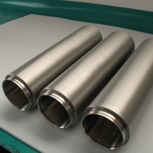
- Precision Machining: We use high-precision machining technology to ensure that the size and shape of the targets meet your strict requirements, allowing for seamless integration into various sputtering systems.
Product Specifications:
To meet the needs of different customers, FOTMA offers molybdenum sputtering targets in various specifications. Here are some common specifications, and we also provide customization services:
- Purity: 99.95% (3N5), 99.97% (3N7), 99.99% (4N) or higher purity, customizable
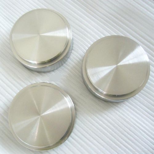
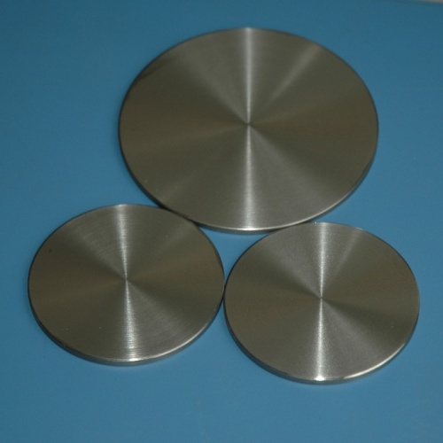
- Shape:
- Circular Targets: Diameter ranging from 50mm to 400mm, or customized
- Square Targets: Side length ranging from 50mm to 500mm, or customized
- Rectangular Targets: Customizable according to customer drawings
- Thickness: 3mm to 25mm, or other customized thicknesses.
- Grain Size: Typically below 50 micrometers (can be controlled according to requirements)
- Surface Roughness: Ra less than 0.8µm (can be polished to a higher surface finish as needed)
- Target Type:
- Bonded Targets: Can be bonded to various backing plate materials, such as copper and aluminum.
- Unbonded Targets: Can be installed and used directly.
- Target Material:
- Molybdenum Alloy Targets (e.g., Mo-Ti, Mo-Nb)
- Doped Molybdenum Targets (e.g., Mo-Al, Mo-Si)
Application Fields:
FOTMA’s high-purity molybdenum sputtering targets are widely used in the following areas:
- Semiconductor Industry: To create barrier layers, contact layers, and thin-film transistors.
- Optical Coating: For the production of optical reflection films, anti-reflection films, and filters.
- Solar Cells: Used as back electrodes and conductive layers.
- Flat Panel Displays: For producing thin film transistors and touch screens.
- Decorative Coating: Providing durable and aesthetically pleasing decorative coatings.
- Other Thin Film Deposition Applications: Including scientific research and industrial production.
Choose FOTMA, and you will receive:
- High-Quality Products: We strictly control every aspect of the process to ensure excellence from raw material to finished product.
- Technical Support: We have a professional team of engineers to provide pre-sales technical consultation and after-sales technical support.
- Customized Services: We can provide customized target specifications and solutions according to your specific needs.
- Reliable Supply: We have a comprehensive production and supply chain management system to ensure timely and stable delivery.
LATEST RECOMMENDED


GET A QUOTE
Send us an Inquiry now to find out more Information and the latest prices,thanks!
Hubei Fotma Machinery Co. Ltd.
Wechat / Whatsapp / Mobile:
+86 13995656368, +86 13907199894
Tel: +86-27-67845266
Email: bunny@fotma.com, export@fotma.com
Address: Guanggu Avenue 52#, Hongshan, Wuhan,
Hubei province, P.R.China. 430074